Silicon Photonics for Intra-Data Centre Communications: Bringing Optics Closer to the Processor
By 2026, the internal architecture of hyperscale data centres has become a decisive factor in overall computing performance. Artificial intelligence workloads, large language models, high-performance computing clusters and real-time analytics have dramatically increased east-west traffic inside server racks. Traditional copper interconnects, once sufficient for 10G and 25G links, now struggle to cope with 400G, 800G and emerging 1.6T data rates. As a result, silicon photonics and advanced optical interconnects are moving physically closer to CPUs, GPUs and AI accelerators. This shift is not experimental; it is already reshaping switch design, transceiver packaging and board-level architectures across leading data centre operators.
Why Copper Is Reaching Its Physical and Economic Limits
Electrical signalling over copper traces faces well-understood physical constraints. As data rates rise beyond 100G per lane, signal attenuation, crosstalk and power consumption increase sharply. Maintaining integrity over even short board-level distances requires complex equalisation and retiming circuits, which add latency and heat. In dense AI servers packed with accelerators, this translates into higher cooling demands and reduced energy efficiency per workload.
Power efficiency has become a central metric for hyperscale operators in 2026. With energy prices volatile and sustainability targets tightening across the UK and EU, the watts per bit consumed by interconnects directly affect operational expenditure. High-speed electrical SerDes operating at 112G and 224G per lane consume significant power, particularly when aggregated across thousands of links inside a single facility.
There is also a mechanical and architectural constraint. Copper cabling and PCB traces require careful routing, shielding and spacing. As switch ASICs approach 51.2 Tbps and 102.4 Tbps capacities, the sheer number of high-speed lanes makes board design increasingly complex. Optical solutions reduce electromagnetic interference and allow longer reach without proportional increases in loss, simplifying layout and enabling higher port density.
Energy Efficiency and Thermal Management as Design Drivers
Thermal management in modern AI racks is no longer a secondary consideration. Direct-to-chip liquid cooling is becoming standard for high-end accelerators, yet interconnect components still contribute a substantial thermal load. Optical links, especially those based on silicon photonics, typically offer lower energy per transmitted bit over comparable distances, reducing the burden on cooling systems.
In 2026, leading transceiver manufacturers report energy efficiencies below 5 pJ/bit for advanced optical modules, with research targets pushing towards 3 pJ/bit. When multiplied across tens of thousands of active links in a hyperscale facility, the cumulative savings are considerable. Lower thermal density also enables tighter rack integration, which is essential for AI training clusters requiring ultra-low latency communication.
From a sustainability perspective, optics closer to the processor aligns with carbon reduction strategies. Reduced electrical losses and improved signal integrity translate into fewer repeaters and less redundant hardware. For operators committed to net-zero targets, interconnect optimisation is now as critical as server efficiency and renewable energy sourcing.
Silicon Photonics and Co-Packaged Optics: A Structural Shift
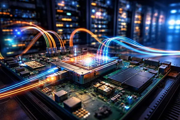
Silicon photonics integrates optical components—such as modulators, waveguides and photodetectors—directly onto silicon substrates using processes compatible with CMOS manufacturing. This compatibility enables large-scale production and tighter integration with switching silicon. By 2026, several major networking vendors have moved from prototype demonstrations to early commercial deployments of co-packaged optics (CPO).
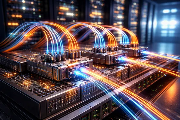
Co-packaged optics place optical engines adjacent to, or within the same package as, the switch ASIC. Instead of routing high-speed electrical signals across the PCB to pluggable transceivers at the front panel, electrical traces are shortened dramatically. The conversion to optical signals happens much closer to the chip, reducing loss, power consumption and latency.
This architectural shift also supports higher aggregate bandwidth. With switch chips reaching beyond 100 Tbps in development roadmaps, traditional pluggable modules face front-panel density constraints. CPO allows optical fibres to connect directly to the switch package via fibre arrays, bypassing some of the physical limitations of faceplate-based designs.
Integration Challenges and Reliability Considerations
Moving optics closer to the processor introduces new engineering challenges. Thermal coupling between hot ASICs and sensitive optical components must be carefully managed. Photonic devices can be temperature-sensitive, affecting wavelength stability and signal quality. Advanced packaging techniques and thermal isolation structures are therefore central to reliable CPO deployment.
Serviceability is another practical issue. Pluggable transceivers are easily replaceable, while co-packaged optics require different maintenance strategies. Vendors are addressing this by modularising optical engines within the package or designing field-replaceable optical sub-assemblies. In 2026, hybrid approaches combining pluggable optics for some ports and CPO for high-density internal fabrics are increasingly common.
Reliability testing has also intensified. Data centre operators demand lifetimes measured in years of continuous operation. Accelerated ageing tests, environmental stress screening and redundant optical paths are now standard in qualification processes. The industry’s experience with 400G and 800G optics has laid the groundwork for scaling to 1.6T without compromising uptime.
Optics Inside the Rack: Board-Level and Chip-to-Chip Links
Beyond rack-to-rack and switch-to-switch connectivity, the next frontier is board-level and even chip-to-chip optical interconnects. AI workloads require massive parallel data exchange between GPUs and accelerators. Electrical interposers and advanced packaging, such as chiplets, have reduced distances, but bandwidth demand continues to rise.
Research and early commercial trials in 2026 focus on optical I/O directly integrated with processor packages. Instead of relying solely on electrical high-speed interfaces, processors may include photonic transceivers at the edge of the package. This approach reduces the need for complex retimers and opens the door to disaggregated architectures, where compute, memory and storage are connected optically within the same rack.
Optical backplanes and fibre-based mid-boards are also under active development. These replace traditional copper backplanes with embedded optical waveguides or fibre ribbons, enabling higher aggregate bandwidth without a proportional increase in power. For hyperscale AI clusters, this supports flatter network topologies and lower latency communication across thousands of nodes.
Implications for Data Centre Architecture in 2026 and Beyond
The move towards optics near the processor is not merely an incremental upgrade; it reshapes data centre design philosophy. Network and compute boundaries are becoming less rigid. Optical fabrics allow resources to be pooled and dynamically allocated, supporting composable infrastructure models that improve utilisation and reduce stranded capacity.
Economically, while initial deployment costs of silicon photonics and CPO remain higher than traditional pluggable optics, total cost of ownership calculations increasingly favour optical integration. Reduced energy consumption, improved density and extended scalability contribute to lower long-term operational expenditure, particularly in AI-centric facilities.
Looking beyond 2026, further advances in integrated lasers, heterogeneous integration and wafer-scale photonics are expected to accelerate adoption. As bandwidth requirements continue to climb, the logic of bringing optics ever closer to the processor becomes difficult to ignore. In modern data centres, light is no longer confined to long-haul links; it is becoming a fundamental building block of internal compute architecture.